- Improved 3D Nanoprinting Technique to Build Nanoskyscrapers
- Name관리자| Date2020-03-26 11:48| Hit1,805
- Attachments Improved 3D Nanoprinting Technique to Build Nanoskyscrapers main pic.jpg (276.4K, 642회)
-
- Simply adding “table salt” helps to build self-stacked nanoarchitectures -
Excerpt from IBS News CenterNanowalls, nanobridges, nano “jungle gyms”: it could seem the description of a Lilliputian village, but these are actual 3D-printed components with tremendous potential applications in nanoelectronics, smart materials and biomedical devices. Researchers at the Center for Soft and Living Matter (CSLM), within the Institute for Basic Science (IBS, South Korea) have improved the 3D nanoprinting process that enables to build precise, self-stacked, tall-and-narrow nanostructures. As shown in their latest publication in Nano Letters, the team also used this technique to produce transparent nanoelectrodes with high optical transmission and controllable conductivity.
The near-field electrospinning (NFES) technique consists of a syringe filled with a polymer solution suspended above a platform, which collects the ejected nanofiber and is pre-programmed to move left-and-right, back-and-forth, depending on the shape of the desired final product. The syringe and the platform have opposite charges, so that the polymer jet coming out from the needle of the syringe is attracted to the platform, forming a continuous fiber that solidifies on the platform. Since the electrospun jets are difficult to handle, this technique was limited to two-dimensional (2D) structures or hollow cylindrical three-dimensional (3D) structures, often with relatively large fiber diameters of a few micrometers.
IBS researchers were able to achieve a better control of the nanofiber deposition on the platform, by adding an appropriate concentration of sodium chloride (NaCl) to the polymer solution. This ensured the spontaneous alignment of the nanofiber layers stacked on top of each other forming walls.
“Although it is highly applicable to various fields, it is difficult to build stacked nanofibers with multiple designs using the conventional electrospinning techniques,” says Yoon-Kyoung Cho, the corresponding author of the study. "Our experiment showed that salt did the trick.”
The benefit provided by salt is related to the charges. The difference in voltage between the syringe and the platform creates positive charges in the polymer solution and negative charges in the platform, but a residual positive charge stays in the solidified fibers on the platform. The team found that applying salt to the polymer solution enhances the charge dissipation, leading to higher electrostatic attraction between the nanofiber jet and the fibers deposited on the platform.
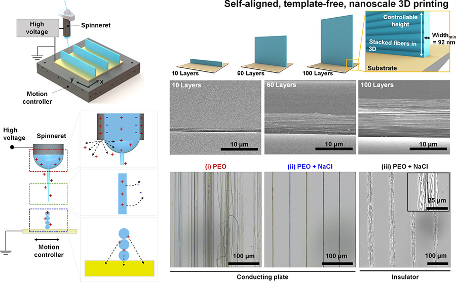
▲ Figure 1: Graphic summary of the study. Near-field electrospinning (NFES) technique and charges. The IBS team achieved precise control of the layer-by-layer nanofiber deposition by just adding salt to the polymer solution. Optical images of the 3D printed nanofibers were prepared with solutions made of: (i) only polymer poly(ethylene oxide) (PEO), (ii) PEO and salt and using a conducting platform, and (iii) PEO and salt using an insulating platform. In (i), the nanostructure is not well aligned, because the deposited fibers have a weak positive surface charge, but adding salt increases the conductivity of the starting solution and the attraction between the nanofiber jet and the deposited fibers. An insulating plate made of silica reduced the effect, confirming the hypothesis. Thanks to this technique, IBS researchers constructed nanowalls with the desired height and number of layers.Based on this mechanism, the team was able to produce tall-and-narrow nanowalls, with a minimum width of around 92 nanometers and a maximum height of 6.6 micrometers, and construct a variety of 3D nanoarchitectures, such as curved nanowall arrays, nano “jungle gyms,” and nanobridges, with controllable dimensions.
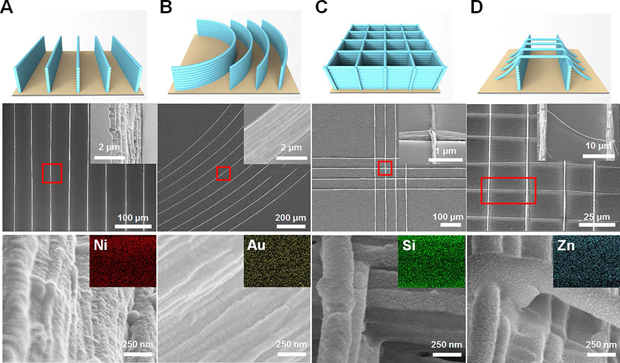
▲ Figure 2: Various 3D printed 40-layer high nanoarchitectures coated with different functional materials. (A) Straight nickel nanowalls. (B) Curved gold nanowalls. (C) Silica grid pattern. (D) Zinc oxide nanobridges suspended between nanowalls.To demonstrate the potential application of these nanostructures, the researchers in collaboration with Hyunhyub Ko, professor at Ulsan National Institute of Science and Technology (UNIST), prepared 3D nanoelectrodes with silver-coated nanowalls embedded in transparent and flexible polydimethylsiloxane (PDMS) films. They confirmed that electrical resistance could be tuned with the number of nanofiber layers (the taller the nanowalls, the smaller the resistance), without affecting light transmission.
“Interestingly, this method can potentially avoid the trade-off between optical transmittance and sheet resistance in transparent electrodes. Arrays of 3D silver nanowires made with 20, 40, 60, 80, or 100 layers of nanofibers had variable conductivity, but stable light transmission of around 98%,” concludes Yang-Seok Park, the first author of the study.
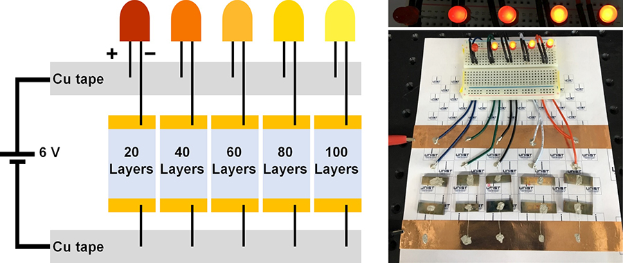
▲ Figure 3: Nanowalls covered with silver and embedded in transparent nanoelectrodes. The setup was used to identify the resistance tunability of the electrodes containing 3D nanowires of different height (from 20 to 100 layers of nanofibers), based on an LED intensity comparison.The Center for Soft and Living Matter is located at Ulsan National Institute of Science and Technology (UNIST).